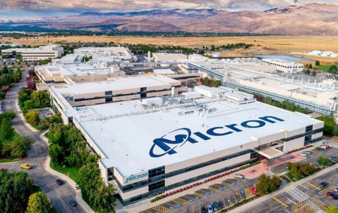
Prime Minister Narendra Modi is scheduled to inaugurate a landmark semiconductor facility in Sanand, Gujarat, on 28 February 2026, marking a major milestone in India’s semiconductor manufacturing journey. The plant, established by Micron Semiconductor Technology India Private Limited, represents one of the largest investments in the country’s high-tech industrial infrastructure and is widely recognised as India’s first advanced semiconductor Assembly, Testing, Marking and Packaging (ATMP) plant.
Valued at ₹22,516 crore, the facility is expected to significantly bolster India’s role in the global semiconductor supply chain by locally transforming raw wafers into finished memory products such as DRAM, NAND and solid-state drives (SSDs). Government and industry officials have described the inauguration as a strategic inflection point for the National Semiconductor Mission, supporting technology self-reliance, employment generation and India’s competitiveness in emerging technologies like artificial intelligence and data infrastructure.
Investment and Strategic Importance
The advanced semiconductor plant at Sanand has been developed with an investment of ₹22,516 crore (approximately USD 2.7 billion) by US-based Micron Technology Inc., through its Indian subsidiary. This investment is among the largest in India’s semiconductor sector and signals significant confidence by global technology companies in the country’s manufacturing ecosystem.
Under its expanded National Semiconductor Mission, the Government of India has been incentivising semiconductor assembly and packaging investments as a strategic priority. The Sanand facility is designed to handle high-end memory products critical to modern computing, enterprise servers and AI-driven systems—segments that have witnessed surging global demand in recent years. Analysts say the plant’s early commissioning puts India on a path to significantly reduce reliance on imports for complex memory components.
Industry experts also point out that this scale of investment serves as a signalling effect for other multinational semiconductor firms evaluating India as a viable manufacturing base. The project’s rapid execution timeline—from approval to inauguration—has strengthened the perception that India can deliver complex, high-precision manufacturing projects within competitive schedules.
Operational Scope, Products and Employment Impact
When fully operational, the Sanand ATMP facility will manufacture fully assembled and packaged memory products, including DRAM (dynamic random-access memory), NAND flash memory and SSD storage solutions that are essential in data centres, smartphones, personal computing devices and AI hardware. These products are expected to meet both domestic demand and global supply requirements.
The plant has already created jobs for roughly 2,000 personnel, including engineers, technicians and support staff. Gujarat state officials project that once the facility reaches full scale, it could generate close to 5,000 direct employment opportunities, contributing to local economic growth and technology skills development. Notably, the company has also emphasised its inclusive employment practices, with specially-abled individuals working as operators and technicians in key operational roles.
Local training institutions have begun collaborating with Micron to design semiconductor-oriented skill programs, indicating a long-term talent pipeline for the sector. These academic-industry linkages are expected to boost India’s specialised workforce capabilities, improving the country’s attractiveness for future semiconductor investments.
Leadership Statements and Industry Backing
Micron Technology’s Chairman, President and CEO Sanjay Mehrotra has highlighted the strategic significance of strong memory and storage systems in modern technologies, especially in artificial intelligence (AI), where rapid data access and performance are critical. Mehrotra remarked that “memory and storage are central to today’s technology,” and added that as AI systems demand faster and more efficient responses, the need for advanced memory infrastructure has become paramount.
State government officials have underscored Gujarat’s leadership role in India’s semiconductor ecosystem. Chief Minister Bhupendra Patel has consistently advocated for fostering a robust technology infrastructure in the state, noting that the Sanand facility exemplifies how coordinated government and corporate partnerships can accelerate critical sector growth. Experts believe that such initiatives are vital for positioning India as a competitive global hub for semiconductor manufacturing.
Industry associations, including the India Electronics and Semiconductor Association (IESA), have welcomed the development, stating that Micron’s entry will serve as a “catalytic anchor investment” capable of attracting suppliers, raw material units, packaging ecosystem players and ancillary industries to Gujarat. This cluster-effect momentum could reshape the state’s industrial profile significantly.
The ATMP Process and Its Role in the Supply Chain
An ATMP facility focuses on the crucial stages of semiconductor production that follow wafer fabrication. After wafers with intricate electronic circuits printed and layered are produced at fabrication plants, they are sent to ATMP facilities for final processing. At the Sanand plant, these wafers will undergo assembly, testing, marking and packaging to become finished memory modules and SSDs ready for market distribution.
The semiconductor manufacturing process begins with the extraction of pure silicon from sand, which is melted and formed into cylindrical ingots. These are sliced into thin wafers that are patterned through advanced photolithography techniques to build millions of transistors. Once chips are created on these wafers, they are separated and sent to the ATMP facility, where they are assembled into packages, tested for performance and reliability, marked with specifications and then packaged for shipment to manufacturers and end users.
The addition of ATMP capabilities in India represents a foundational step toward developing a full-stack semiconductor ecosystem. Though wafer fabs remain the next major target, having a world-class packaging and testing infrastructure enables India to participate meaningfully in global supply chains, strengthening resilience against geopolitical disruptions.
Broader Implications for India’s Tech Ecosystem
The Sanand ATMP plant is a key pillar of India’s ambition to cultivate a vibrant semiconductor ecosystem, which includes future fabrication facilities and a comprehensive supply chain. By localising advanced packaging and testing capabilities, India aims to strengthen its position in critical technology sectors, decrease import dependency and attract further foreign and domestic investments.
Industry analysts argue that this development could pave the way for larger wafer fabrication units in the future, potentially under initiatives such as the India Semiconductor Mission’s incentives for fully integrated fabs. Such progress would have far-reaching impacts on India’s electronics manufacturing landscape and support the broader “Make in India” vision in high-technology sectors.
The project also strengthens India’s geopolitical standing, particularly as global powers compete to secure diversified chip supply chains. With major economies seeking alternatives beyond East Asia, India’s entry as a credible semiconductor destination could redefine its role in strategic global technology partnerships.